
Add to Favorites


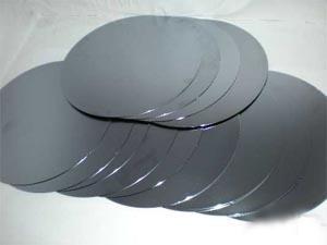
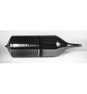
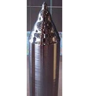
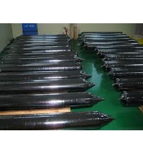
P Type Monocrystalline Silicon Wafer
-
Payment


-
Origin
China Mainland
-
Minimum Order
5
-
Packing
Pieces
- Contact Now Start Order
- Description
Product Detail
Silicon wafers are used as a substrate material in a wide range of applications. They are the building block of modern electronics. We offers Prime, Test, Monitor, SEMI standard, and customized silicon wafers in all diameters from 100mm to 400mm. Our silicon wafers are made by the most commonly used process called Czochralski (CZ) process.
Our Capability | Diameter | Orientation | Type | Dopant | Thickness | Resistivity |
Specification | 100 to 300 mm or custom sizes | 1-0-0, 1-1-1, 1-1-0 | P | Boron | custom sizes | 0.0006- 200ohm-cm |
You May Like
-
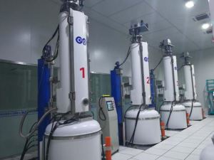
Silicon Crystal Growth Furnace 1500 5 Pieces / (Min. Order)

-
Silicon Crystal Growth Furnace 1200 5 Pieces / (Min. Order)

-
Silicon Crystal Growth Furnace 1050 5 Pieces / (Min. Order)
-
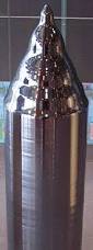
<110> Oriented Silicon Ingot 5 Pieces / (Min. Order)
-
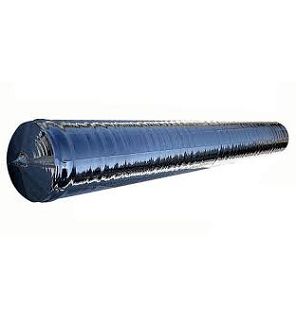
Ultra-high Doped Monocrystalline Silicon Ingot 5 Pieces / (Min. Order)
-
High Doped Monocrystalline Silicon Ingot 5 Pieces / (Min. Order)
-
Lightly Doped Monocrystalline Silicon Ingot 5 Pieces / (Min. Order)

-
Antimony Doped Monocrystalline Silicon Ingot 5 Pieces / (Min. Order)
-
Phosphorus Doped Monocrystalline Silicon Ingot 5 Pieces / (Min. Order)

-
P Type Monocrystalline Silicon Ingot 5 Pieces / (Min. Order)
Not exactly what you want? One request, multiple quotations Get Quotations Now >>
 Favorites

You May Like
-
Silicon Crystal Growth Furnace 1500
5 Pieces / (Min. Order)
-
Silicon Crystal Growth Furnace 1200
5 Pieces / (Min. Order)
-
Silicon Crystal Growth Furnace 1050
5 Pieces / (Min. Order)
-
<110> Oriented Silicon Ingot
5 Pieces / (Min. Order)
-
Ultra-high Doped Monocrystalline Silicon Ingot
5 Pieces / (Min. Order)
-
High Doped Monocrystalline Silicon Ingot
5 Pieces / (Min. Order)
-
Lightly Doped Monocrystalline Silicon Ingot
5 Pieces / (Min. Order)
-
Antimony Doped Monocrystalline Silicon Ingot
5 Pieces / (Min. Order)
-
Phosphorus Doped Monocrystalline Silicon Ingot
5 Pieces / (Min. Order)
-
P Type Monocrystalline Silicon Ingot
5 Pieces / (Min. Order)